HALF MOON BAY, Calif. – January 11, 2011 – SEMI today named Thomas DiStefano, John W. Smith, Jr. and Michael Warner as recipients of the SEMI Award for North America for contributions to the development and commercialization of Micro Ball Grid Array (μBGAÒ ) technology. This advancement led to many forms of semiconductor chip scale packaging that enabled cost effective miniaturization. It has had a significant impact on the proliferation of products with smaller form factors, such as handheld phones, recorders, games and other electronics that have since become common. The SEMI Award for North America is the association’s highest honor for technical contribution to the semiconductor industry. The industry awards will be presented during a banquet at the 2011 SEMI Industry Strategy Symposium (ISS) in Half Moon Bay, California this evening.

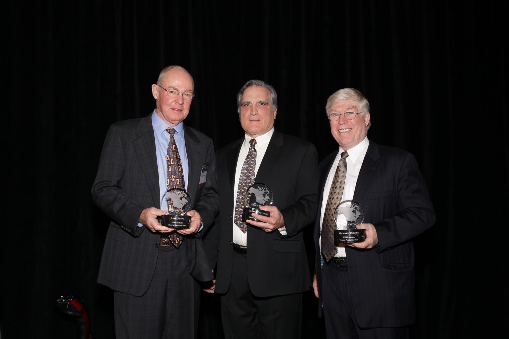
Recipients John Smith, Tom Di Stefano, and Mike Warner
“Our industry honors Tom DiStefano, John Smith and Michael Warner for their combined efforts to commercialize Micro Ball Grid Array technology while at Tessera Technologies,” said Stanley T. Myers, president and CEO of SEMI. “This critical packaging technology was an important development in the proliferation of smaller personal electronic devices that have spurred the market for semiconductor devices.”

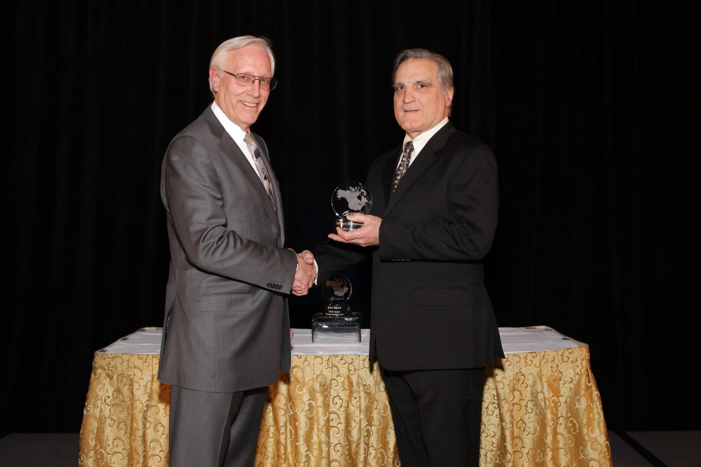
Bill Bottoms presenting award to Tom Di Stefano
Dr. DiStefano was the founding president of Tessera Technologies and a co-founder of ChipScale Review. DiStefano helped to build Tessera into a world leader in miniaturized packaging. Royalties from U.S. Patents coauthored by DiStefano produced well above $1Billion revenue for Tessera. John W. Smith, Jr. joined Tessera in 1992 as its CEO where he served until his retirement in 2000. Michael Warner, a Tessera Fellow, joined the company in 1994 as the corporate officer responsible for developing products employing µBGA solutions for government, medical and commercial applications.
“The introduction of chip scale packaging enabled a decrease in package size and an increase in package frequency while reducing the total power required,” said Bill Bottoms, chairman of the SEMI Award Advisory Committee. “This innovation is now the packaging solution of choice for most memory devices and a significant number of logic devices. It was initially adapted to meet performance requirements and the high-volume commercialization led to its widespread adaption as a lower-cost packaging alternative.”
The SEMI Award was established in 1979 to recognize outstanding technical achievement and meritorious contribution in the areas of Semiconductor Materials, Wafer Fabrication, Assembly and Packaging, Process Control, Test and Inspection, Robotics and Automation, Quality Enhancement, and Process Integration.
The award is the highest honor conferred by SEMI. It is open to individuals or teams from industry or academia whose specific accomplishments have broad commercial impact and widespread technical significance for the entire semiconductor industry. Nominations are accepted from individuals of North American-based member companies of SEMI. Past award recipients include Walter Benzing and Mike McNealy, Ken Levy, Jean Hoerni, Dan Maydan, Robert Akins and Igor Khandros, among others.
About SEMI
SEMI is the global industry association serving the manufacturing supply chains for the microelectronic, display and photovoltaic industries. SEMI member companies are the engine of the future, enabling smarter, faster and more economical products that improve our lives. Since 1970, SEMI has been committed to helping members grow more profitably, create new markets and meet common industry challenges. SEMI maintains offices in Austin, Beijing, Bengaluru, Berlin, Brussels, Grenoble, Hsinchu, Moscow, San Jose, Seoul, Shanghai, Singapore, Tokyo, and Washington, D.C. For more information, visit www.semi.org.
Association Contact
Deborah Geiger/SEMI
Tel: 1.408.943.7988
E-mail: dgeiger@semi.org


It’s really a great and helpful piece of information. I
am glad that you shared this useful information with us.
Please keep us informed like this. Thank you for sharing.